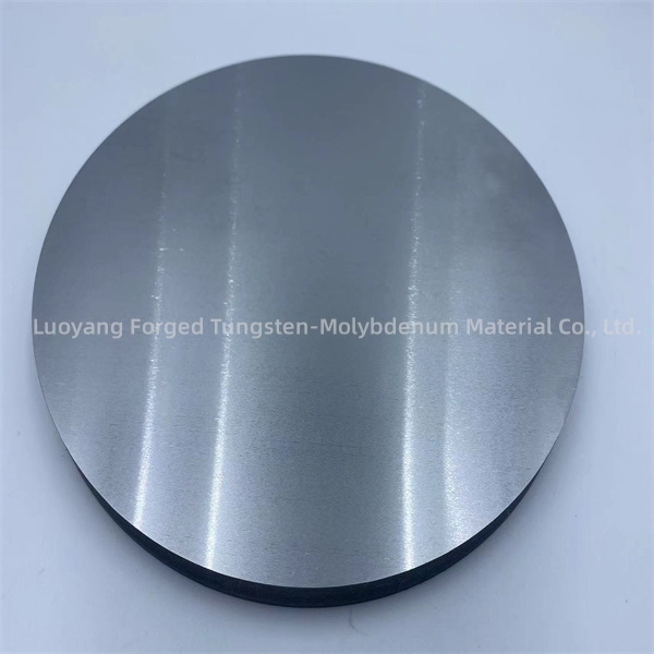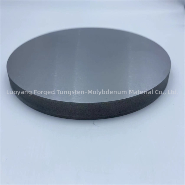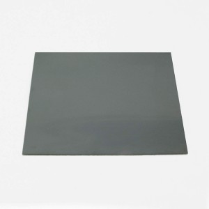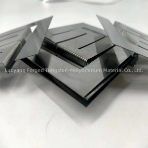
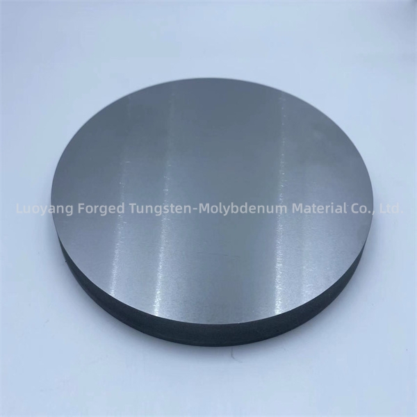
Molybdenum target material widely used in the semiconductor field
1. The purity of molybdenum powder is greater than or equal to 99.95%. Densification treatment of molybdenum powder was carried out using hot pressing sintering process, and the molybdenum powder was placed in the mold; After placing the mold into the hot pressing sintering furnace, vacuum the hot pressing sintering furnace; Adjust the temperature of the hot press sintering furnace to 1200-1500 ℃, with a pressure greater than 20MPa, and maintain the insulation and pressure for 2-5 hours; Forming the first molybdenum target billet;
2. Perform hot rolling treatment on the first molybdenum target billet, heat the first molybdenum target billet to 1200-1500 ℃, and then perform rolling treatment to form the second molybdenum target billet;
3. After hot rolling treatment, the second molybdenum target material is annealed by adjusting the temperature to 800-1200 ℃ and holding it for 2-5 hours to form a molybdenum target material.
Molybdenum targets can form thin films on various substrates and are widely used in electronic components and products.
Performance of Molybdenum Sputtered Target Materials
The performance of molybdenum sputtering target material is the same as that of its source material (pure molybdenum or molybdenum alloy). Molybdenum is a metal element mainly used for steel. After industrial molybdenum oxide is pressed, most of it is directly used for steelmaking or cast iron. A small amount of molybdenum is smelted into molybdenum iron or molybdenum foil and then used for steelmaking. It can improve the strength, hardness, weldability, toughness, as well as high temperature and corrosion resistance of alloys.
Application of Molybdenum Sputtering Target Materials in Flat Panel Display
In the electronics industry, the application of molybdenum sputtering targets is mainly focused on flat panel displays, thin-film solar cell electrodes and wiring materials, as well as semiconductor barrier layer materials. These materials are based on high melting point, high conductivity, and low specific impedance molybdenum, which has good corrosion resistance and environmental performance. Molybdenum has the advantages of only half the specific impedance and film stress of chromium, and has no environmental pollution issues, making it one of the preferred materials for sputtering targets in flat panel displays. In addition, adding molybdenum elements to LCD components can greatly improve the brightness, contrast, color, and lifespan of the LCD.
Application of Molybdenum Sputtering Target Materials in Thin Film Solar Photovoltaic Cells
CIGS is an important type of solar cell used to convert sunlight into electricity. CIGS is composed of four elements: copper (Cu), indium (In), gallium (Ga), and selenium (Se). Its full name is copper indium gallium selenium thin film solar cell. CIGS has the advantages of strong light absorption capacity, good power generation stability, high conversion efficiency, long daytime power generation time, large power generation capacity, low production cost, and short energy recovery period
Molybdenum targets are mainly sprayed to form the electrode layer of CIGS thin film batteries. Molybdenum is located at the bottom of the solar cell. As the back contact of solar cells, it plays an important role in the nucleation, growth, and morphology of CIGS thin film crystals.
Molybdenum sputtering target for touch screen
Molybdenum niobium (MoNb) targets are used as conductive, covering, and blocking layers in high-definition televisions, tablets, smartphones, and other mobile devices through sputtering coating.
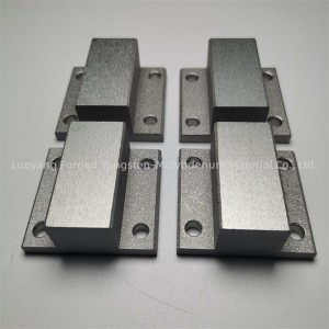
| Product Name | Molybdenum target material |
| Material | Mo1 |
| Specification | Customized |
| Surface | Black skin, alkali washed, polished. |
| Technique | Sintering process, machining |
| Meltng point | 2600℃ |
| Density | 10.2g/cm3 |
Wechat:15138768150
WhatsApp: +86 15236256690
E-mail : jiajia@forgedmoly.com